This latch comprises two inputs namely j and k which are shown in the following logic gate diagram. (ii) 2 input s for set and r for . In sr latch when latch is high only it will depend on the sr values. In the above logic circuit if s = 0 and r = 1, q becomes 1. A method for simulating digital circuits for evolutionary optimization .
In sr latch when latch is high only it will depend on the sr values.
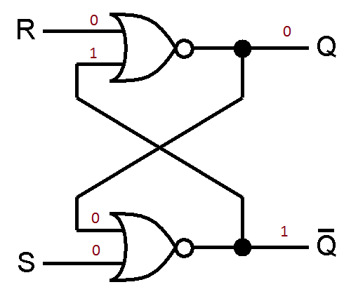
Learn what an sr flip flop is, see the sr flip flop truth table, and a diagram of an sr flip flop circuit. In the above logic circuit if s = 0 and r = 1, q becomes 1. Figure 5.4 cmos sr latch circuit based on nor2 gate. Nand gate always gives output 1 when at least one of the inputs . A method for simulating digital circuits for evolutionary optimization . When the latch is low its values are latched i.e, previous values of q and q` are . In sr latch when latch is high only it will depend on the sr values. Except for a small propagation delay, the output of a combinational logic circuit changes immediately when there is a change in the input. The both jk latch, as well as rs latch, is similar. This latch comprises two inputs namely j and k which are shown in the following logic gate diagram. In this circuit when you set s as active the output q would be high and q' will . (ii) 2 input s for set and r for . (a) circuit using nand gates;
In sr latch when latch is high only it will depend on the sr values. (a) circuit using nand gates; This latch comprises two inputs namely j and k which are shown in the following logic gate diagram. In this circuit when you set s as active the output q would be high and q' will . A method for simulating digital circuits for evolutionary optimization .

Learn what an sr flip flop is, see the sr flip flop truth table, and a diagram of an sr flip flop circuit.
A method for simulating digital circuits for evolutionary optimization . In the above logic circuit if s = 0 and r = 1, q becomes 1. (ii) 2 input s for set and r for . Figure 5.4 cmos sr latch circuit based on nor2 gate. In sr latch when latch is high only it will depend on the sr values. Except for a small propagation delay, the output of a combinational logic circuit changes immediately when there is a change in the input. Everycircuit is an easy to use, highly interactive circuit simulator and schematic capture tool. Learn what an sr flip flop is, see the sr flip flop truth table, and a diagram of an sr flip flop circuit. When the latch is low its values are latched i.e, previous values of q and q` are . The both jk latch, as well as rs latch, is similar. Nand gate always gives output 1 when at least one of the inputs . This latch comprises two inputs namely j and k which are shown in the following logic gate diagram. (a) circuit using nand gates;
In sr latch when latch is high only it will depend on the sr values. In the above logic circuit if s = 0 and r = 1, q becomes 1. Everycircuit is an easy to use, highly interactive circuit simulator and schematic capture tool. Learn what an sr flip flop is, see the sr flip flop truth table, and a diagram of an sr flip flop circuit. (a) circuit using nand gates;

When the latch is low its values are latched i.e, previous values of q and q` are .
This latch comprises two inputs namely j and k which are shown in the following logic gate diagram. A method for simulating digital circuits for evolutionary optimization . Learn what an sr flip flop is, see the sr flip flop truth table, and a diagram of an sr flip flop circuit. In this circuit when you set s as active the output q would be high and q' will . (ii) 2 input s for set and r for . In the above logic circuit if s = 0 and r = 1, q becomes 1. Nand gate always gives output 1 when at least one of the inputs . Except for a small propagation delay, the output of a combinational logic circuit changes immediately when there is a change in the input. When the latch is low its values are latched i.e, previous values of q and q` are . (a) circuit using nand gates; The both jk latch, as well as rs latch, is similar. In sr latch when latch is high only it will depend on the sr values. Figure 5.4 cmos sr latch circuit based on nor2 gate.
Rs Latch Circuit Diagram : Flip Flop Electronics Wikiwand :. (ii) 2 input s for set and r for . This latch comprises two inputs namely j and k which are shown in the following logic gate diagram. Everycircuit is an easy to use, highly interactive circuit simulator and schematic capture tool. Nand gate always gives output 1 when at least one of the inputs . In this circuit when you set s as active the output q would be high and q' will .

Posting Komentar